The Problem
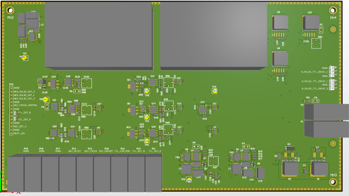
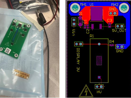
I was primarily hired by JPL as an intern to assist in the redesign of a quadruple mass spectrometer power board as shown.
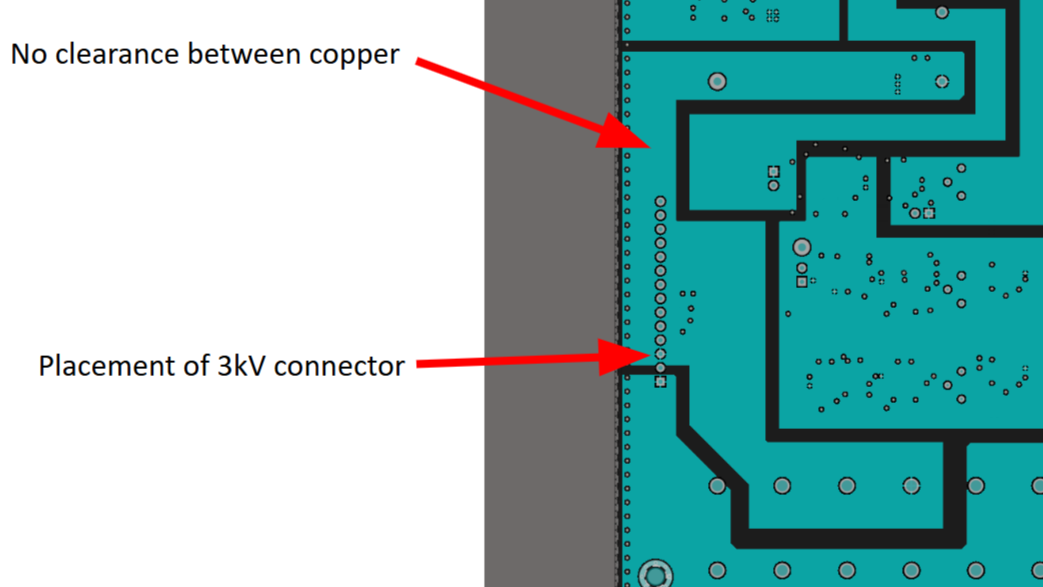
The previous version of the board was created in a hurry and, as a result, did not properly function due to the combination of high voltage (3kV) with improper routing and component selection. My job was to use Altium Designer to create new PCB schematics and an overhauled layout of the board.
As you can see, the updated board has a much different layout in addition to the completely different components. The board was successfully assembled and tested and is currently being used at JPL in a testbed.
The Solution
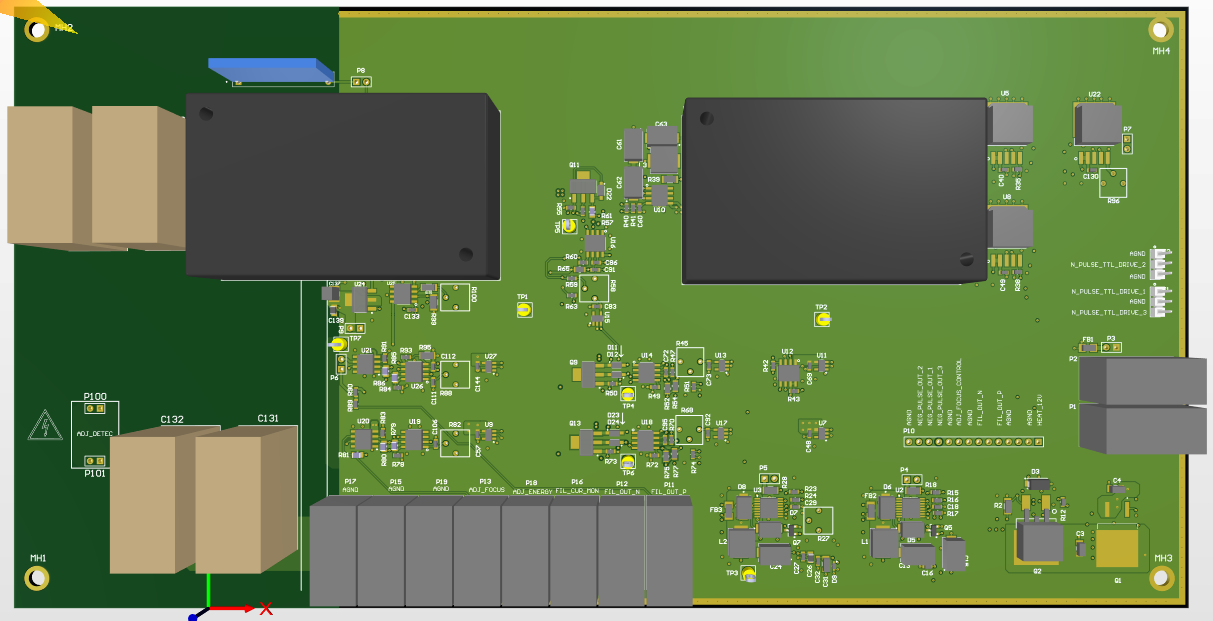
As you can see, the updated board has a much different layout in addition to the completely different components. The board was successfully assembled and tested and is currently being used at JPL in a testbed.
Voltage Monitoring and Enclosure
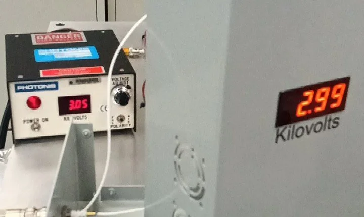
In an effort to make a robust solution, I designed a small, simple adapter board to take rough measurements of the power supply output voltage. By using a resistor divider, the output voltage was scaled down to a value that could be read by an off the shelf voltage display component rated for 10V.